Final ddr3 memory layout & length calculator spreadsheet Ddr2 layout example ddr3 examples pcb ddr x16 rank Ddr ddr2 hynix specification
memory - DDR1 Layout Considerations - DOs and DONTs - Electrical
Fly-by topology routing for ddr3 and ddr4 memory Watch routing pcb layout with ddr3 & high speed interfaces Main design guidelines & layout rules on high speed printed circuit
Ddr3 pcb bga impedance routing kicad zynq
Pcb layout for manufacturing (dfm)Pcb layout memory ddr3 fast Topology routing ddr ddr3 ddr4 pcb altiumPcb layout fast forward.
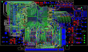
Ddr layout routing pcb plan memory successful settingDdr, ddr2 and ddr3 How to plan for ddr routing in pcb layoutDdr, ddr2 and ddr3 – pcb layout examples – welldone blog.

Pcb layout ddr layer hs
Ddr3 ddr ddr2 smd corners fiducialsDdr memory module pcb design specification(ddr2 fbdimm, hynix How to route ddr3 memory and cpu fan-outDdr3 route memory cpu fanout pcb fan altium groups designer space closest routed left under figure used.
Ddr pcb delay propagation eevblogRouting pcb ddr3 interface feel while imgur comments ics rotated board ece squiggly tracks those make Ddr3 length spreadsheet rex imx6 signals finishedPcb layout high speed ddr.

Dl designs
Pcb routing layout ddr3 speed high interfacesA large bga, ddr3, & impedance control on a 6-layer pcb · craig j. bishop Ddr3 pcb design routingPcb design.
Memory considerations ddr1 dos donts layout completion checklist entire after electricalRouting pcb ddr3 power sdram stack .

PCB Layout for Manufacturing (DFM) | San Francisco Circuits

Watch routing PCB Layout with DDR3 & High Speed Interfaces - YouTube

How to Plan for DDR Routing in PCB Layout

Fly-by Topology Routing for DDR3 and DDR4 Memory | PCB Design Blog | Altium

A large BGA, DDR3, & impedance control on a 6-layer PCB · Craig J. Bishop

DDR memory module PCB design specification(DDR2 FBDIMM, HYNIX

memory - DDR1 Layout Considerations - DOs and DONTs - Electrical

DDR, DDR2 and DDR3 - PCB layout examples - Welldone Blog - FEDEVEL

DDR3 pcb design routing - Electrical Engineering Stack Exchange